


ABSTRACT
F4PGA is an open-source FPGA toolchain designed as a free alternative to proprietary computer-aided design tools like Xilinx’s Vivado. Currently, mapping designs to DSP blocks and generating DSP block bitstreams are not implemented for the Xilinx 7-series FPGA devices within the toolchain. This project aims to integrate DSP48E hard block in F4PGA. This will enable designs using DSPs to be synthesized, placed, and routed correctly. We need to diagnose and implement changes needed throughout the F4PGA toolchain, allowing for DSP design bitstreams to be successfully generated with open-source tools. I have first presented an overview of the working of the F4PGA toolchain. Subsequently, I have shared my implementation strategy along with the timeline for the project.
DELIVERABLES
i. Support for DSP48E within the F4PGA architecture definitions.
ii. Testing flow for designs using Xilinx 7-series DSP hard blocks which include,
Verilog-to-Bitstream using the F4PGA toolchain.
Fasm2bels to re-generate the original netlist from the bitstream output of F4PGA.
Proof-test through Vivado to verify the correctness of the netlist.
iii. Updated F4PGA Documentation
iv. Progress reports every two weeks to let my mentor know the latest status of the project.
Proposed stretch goals:
i. Improve Project X-Ray so that it can use new Vivado versions. (prjxray only supports Vivado 2017.2 currently)
ii. Add support for new FPGA architectures.
INTRODUCTION
a. Overview of F4PGA
F4PGA is a fully open-source toolchain for the development of FPGAs of multiple vendors. It is a workgroup under the CHIPS Alliance, which aims to provide an open-source solution for HDL to FPGA bitstream synthesis. To establish a comprehensive end-to-end flow for FPGA development, a range of tools and projects are required. This includes logic synthesis and implementation tools, as well as chip documentation projects that cater to the needs of various FPGA vendors. These different components work together to provide a complete F4PGA toolchain that enables rapid prototyping and software-driven development of FPGA-oriented systems. Currently, it is targeting Xilinx’s 7-Series, QuickLogic’s EOS-S3, and Lattice’s iCE40 and ECP5 FPGAs.
b. Problem statement
Modern FPGAs are equipped with multiple pre-designed and pre-optimized hard-blocks. These blocks are usually designed for specific functions such as arithmetic operations, digital signal processing, memory, and high-speed serial interfaces, and are highly optimized for their intended purpose. The advantage of using hard blocks is that they are highly efficient and can perform their intended functions much faster than if the same logic were implemented using the FPGA fabric. Using hard blocks can also free up the fabric for other tasks, as it reduces the number of resources required to implement a specific function.
The goal of this project is to incorporate support for the DSP48E hard block of Xilinx 7-series FPGA devices in the F4PGA toolchain. Preparing a working bitstream for a particular FPGA chip involves generating a description of the FPGA chip, which includes timing and resource information, and techmaps for synthesis tools, by utilizing relevant bitstream documentation (Project X-Ray documents the Xilinx 7-Series FPGA architecture). The DSP hard block of the Xilinx 7-series FPGA devices (DSP48E) is currently documented in Project X-Ray, but it currently lacks support within the F4PGA architecture definitions. With the addition of the required support for DSP48E to the architecture definition, the designs that use DSPs can be synthesized, placed, and routed accurately. In addition, the project aims to ensure the successful completion of the testing flow for Xilinx 7-series DSP hard block designs.
c. Technical details
This section provides a description of the F4PGA toolchain. The following diagram illustrates the F4PGA tooling ecosystem targeting the Xilinx 7-series FPGA devices.
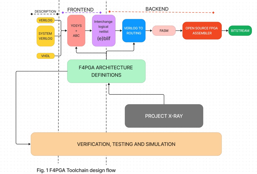
The toolchain involves creating a description of the chip's resources and timings (within the F4PGA architecture definitions), Verilog to netlist synthesis in Yosys, implementation using Verilog to Routing (VTR), and finally translating design properties into a set of features saved in FASM format and then into a bitstream using relevant bitstream documentation projects.
Yosys converts Verilog designs into a flattened netlist, which includes logic gates, flip-flops, and blackboxes representing various blocks such as adders, multipliers, and RAM slices. The process of synthesis involves using a package called ABC, which performs technology-independent logic optimization and maps the circuit into Look Up Tables (LUTs), flip-flops, and blackboxes. Following this, a technology mapping pass is performed by Yosys to transform the primitives generated by Yosys into those that are compatible with VPR. This requires appropriate techmaps to guide Yosys in translating the primitives to the versions that align with the F4PGA architecture definitions.
Once the synthesis process is completed, the next step is to implement the design on the target FPGA device. This involves the use of placement and routing tools, which are responsible for assigning physical locations to individual blocks from the synthesis description and creating connections between them. For F4PGA, Verilog to Routing (VTR) is the chosen tool for this task. VTR takes in a description of the FPGA architecture and a technology-mapped user circuit as input. It performs packing, placement, and routing to map the circuit onto the FPGA and generates the FPGA configuration needed to implement the circuit as output.
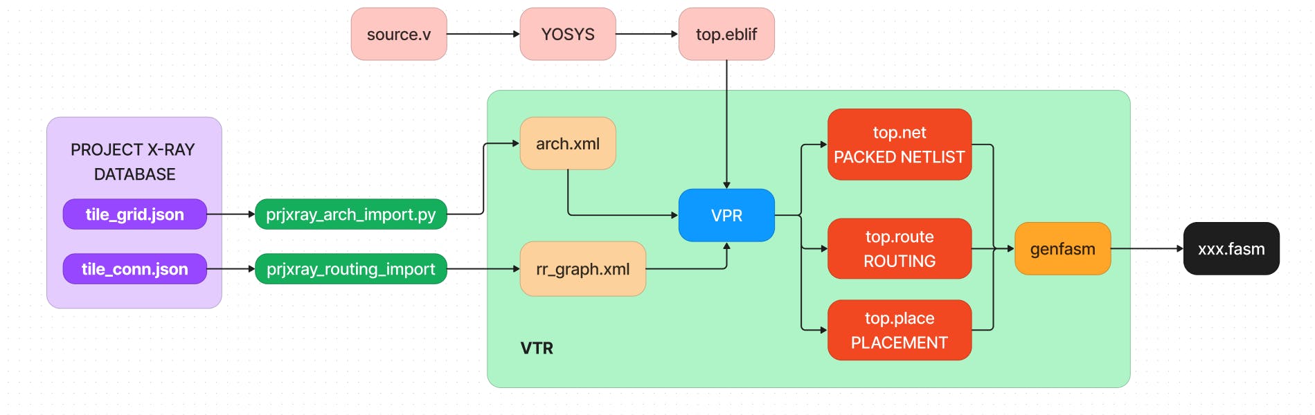
The importance of the "F4PGA architecture definitions" as the core resources in the toolchain is apparent. This undertaking encompasses valuable materials, both human-readable and machine-readable, that outline the basics and routing structure for diverse FPGA architectures. In order to facilitate the integration of a specific primitive into VTR, two files are required within the architecture definitions:
Model XML (xxx.model.xml) which contains general information about the module’s input and output ports and their relations.
Physical Block XML (xxx.pb_type.xml) - Describes the actual layout of the primitive, with information about the timings, internal connections, etc.
Techmaps for Yosys can then be prepared correctly using these primitives.
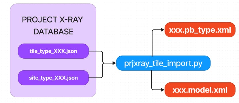
If a block is already documented in the Project X-Ray, “prjxray_tile_import.py” can be used to generate the pb_type.xml and model.xml files of the corresponding primitive.
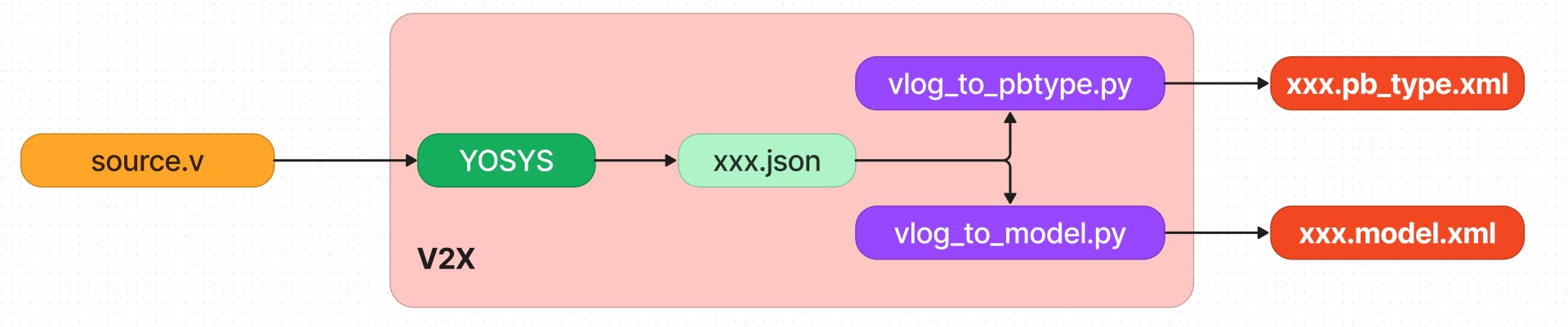
V2X can also be used to generate .pb_type.xml and .model.xml files from Verilog sources using the utilities in “f4pga-v2x”.
To add a new family of FPGA to Project X-Ray, multiple steps are involved. The process follows a "black box" approach, where Vivado generates a vast number of designs that are utilized to create bitstreams. The cross-correlation of resulting bitstreams is then performed to understand the functionality of different bits. Fuzzers play a significant role in this process by generating a set of tests that help reverse-engineer the FPGA architecture. Finally, the accuracy of the reverse-engineered architecture is tested and necessary adjustments are made.
IMPLEMENTATION PLAN
a. Update model and physical block type definitions
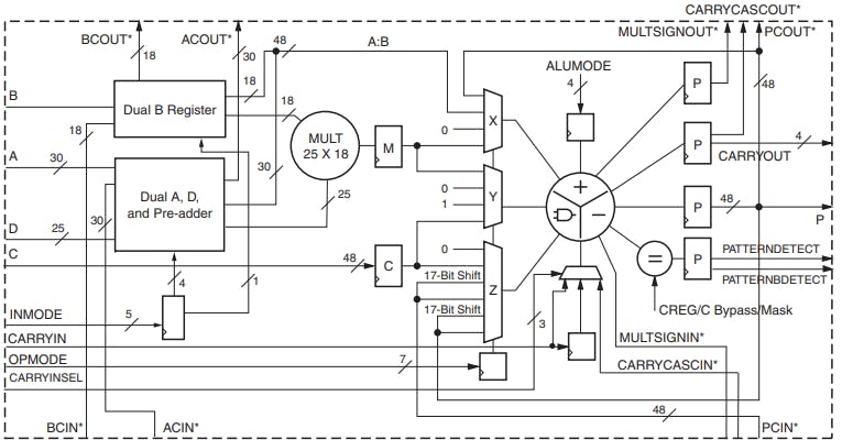
The routing graphs and architecture files for a desired FPGA are utilized in VTR. These files need to be updated to support DSP48E block. Vendor specific FPGA primitives are defined within the F4PGA architecture definitions repository. These primitives (consisting of pb_type.xml and model.xml files) can be thought of as the building blocks for their target architecture that can produce routing graphs and architecture files for a desired FPGA. Develop a DSP48E primitive using XILINX documentation. The following figure shows the internal structure of a DSP48E block:
Since the DSP48E is already documented in the Project X-Ray database, its primitive can be developed using the utility <prjxray_tile_import.py>.
Add pb_type.xml and model.xml for the DSP48E block at the following location within the repository: <f4pga-arch-defs/xilinx/common/primitives/dsp48e1/>
Update the cmake files to include the newly added primitive to the architecture. Make appropriate changes in the Yosys tcl scripts to enable the synthesis of DSP slices.
b. Add DSP tiles to target architectures
Add DSP_L and DSP_R tiles to < f4pga-arch-defs/xilinx/xc7/archs/artix7_/tiles/>.
These tiles are documented within the Project X-ray database. To enable a new tile/pb_type in a target device, update the CMakeLists.txt within: < f4pga-arch-defs/xilinx/xc7/archs/artix7_/devices/xc7a**t-virt/>
c. Generate Routing Graph and Architecture File
After creating all desired primitives and tile definitions for the target architecture, run “make env” for the directory. This command will create a new build directory that contains copies of the primitive and tile definitions, along with the framework for creating routing graphs and architecture files. By the end of this process, files will have been generated using the primitive and tile definitions for the Artix-7. The most notable of these files are the newly created routing graph and architecture file.
d. Update Yosys techmaps
To allow VPR to elaborate Yosys output netlist, we need to perform a technology mapping pass to transform the Yosys-generated primitives to the VPR-compatible ones. To do so modify cells_map.v and cells_sim.v in < f4pga-arch-defs/xilinx/xc7/techmap/>. They are necessary to translate the gate level netlist that is output from Yosys onto a set of VPR-readable cells that can be packed, placed, and routed onto the FPGA. Add a DSP48E module to <cells_map.v> that maps to DSP48E_VPR defined in the <cell_sim.v>. “cell_map.v” defines how specific cells need to be re-mapped and “cell_sim.v” defines the VPR-specific cells that will be present in the .eblif output.
Expand these VPR libraries to allow for the behavioral modeling (apart from structural modeling) of DSP48E1 instances while maintaining necessary parameter values and GND/VCC connections. With this change, Yosys synthesis could map a DSP block with all needed parameters with RTL input such as “AB”, creating a functioning multiplier without explicitly setting port inputs, outputs, and parameters. Errors might arise after making all the changes described above. Check all the utilities involved in the toolchain, and make necessary modifications to enable support for DSP blocks.
e. Add tests for Xilinx 7-series DSP hard blocks
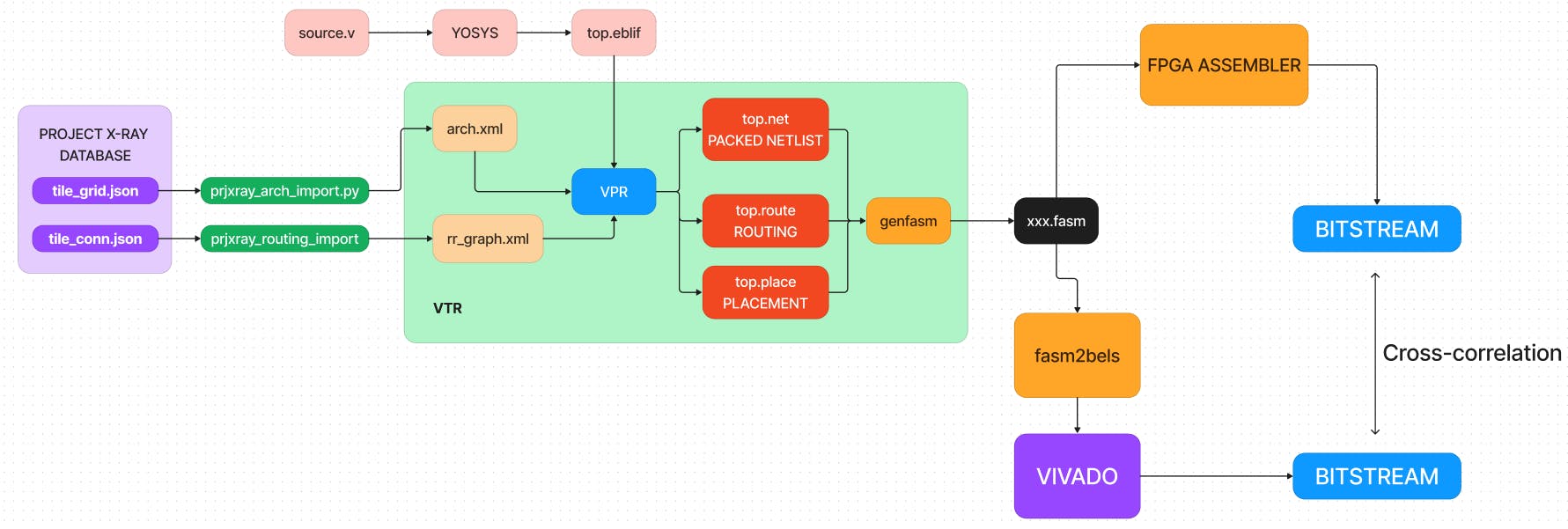
Add tests in < f4pga-arch-defs/xilinx/xc7/tests/> to verify the correctness of newly added support for DSP block. This can be done by cross checking the bitstream generated by the F4PGA with Vivado. The following diagram illustrates this:
The DSP block supports several independent functions, such as addition/subtraction, multiplication, shifting, magnitude comparison, pattern detection, and counting. Add sources.v in tests such that it leads to verification of all the functionality of the DSP48E block.
f. Update documentation
All the changes and additions to the toolchain so far need to be documented. Update all the required documentation under the F4PGA project.
TIMELINE AND MILESTONES
• Community Bonding Period (May 4 – May 28)
Research and familiarize with the project.
Extensively read the documentation for f4pga, VTR, and Yosys.
Read Xilinx documentation for DSP48E.
Understand the various projects under the f4pga toolchain while addressing issues in their repositories.
Discuss the feasibility of the proposed timeline with the mentors and make necessary changes based on their inputs.
• Phase 1
Week 1 and 2 (May 29 – June 11)
Develop DSP48E1 primitive by referring to the official documentation of Xilinx 7 series FPGAs and reverse engineered architecture available in the Project X-Ray database.
Submit progress report 1 to mentor.
Week 3 (June 12 – June 18)
Make appropriate changes in the Yosys tcl scripts to enable the synthesis of DSP slices.
Add DSP tiles to target architectures.
Update the cmake files to include the newly added primitive to the architecture.
Re-generate the routing graph and architecture file for VPR.
Week 4 and 5 (June 19 – July 2)
Update Yosys techmaps to enable support for DSP48E1 primitive.
User will be able to generate bitstreams for designs that contain dsp elements defined structurally within the RTL code.
Expand VPR libraries to allow behavioral modeling of DSP elements.
Submit progress report 2 to mentor.
Week 6 (July 3 – July 9)
This week will be used as a buffer.
Update relevant documentation.
Debug any bugs or errors that may have occurred.
• Midterm Evaluation (July 10 – July 14)
Submit the midterm evaluations.
• Phase 2
Week 7 and 8 (July 10 – July 23)
Create multiple test Verilog design sources covering all the functionality of the DSP48E block.
These tests will then be used in Verilog to bitstream conversion using the F4PGA toolchain.
Verify the generated bitstreams by uploading them into an FPGA or using FPGA emulators available online.
Submit progress report 3 to mentor.
Week 9 and 10 (July 24 – Aug 6)
Use the tests that were generated earlier to generate bitstreams using F4PGA. Now use fasm2bels to regenerate the netlist from FASM. Process this netlist through Vivado and generate bitstreams. The two bitstreams generated need to be cross checked for errors in the F4PGA output.
Identify the sources of errors. Modify the architecture definition of DSP48E1 primitive or Yosys techmap libraries and iterate this step until the bitstreams are identical.
Week 11 (Aug 7 – Aug 13)
Continue testing and improvising.
Code clean-up.
Integrate the project in the main F4PGA repository.
Resolve issues faced by the community.
Submit progress report 4 to mentor.
Week 12 (Aug 14 – Aug 20)
This week will be used as a buffer.
Update relevant documentation.
Discuss the extension of the project with the mentor to incorporate certain stretch goals.
Prepare a timeline for the extended project period after consulting with the mentor.
• Final Evaluation (Aug 21 – Aug 28)
Submit the final work product and final mentor evaluation.
• Extended Timeline (Sep 4 – Nov 6)
I am willing to extend the proposed timeline to work on stretch goals. The extended duration as well as the targeted stretch goals will have to be decided upon after discussion with the mentor.
PERSONAL DETAILS
a. Basic info
Name: Abhishek Anand
Major: Electronics and Communication Engineering
Degree: Bachelor of Technology
Year: Junior (3rd or pre-final)
University: National Institute of Technology, Durgapur
Slack Handle: ABHISHEK ANAND
Personal Email: anand.dark.aster@gmail.com
University Email: aa.20u10582@btech.nitdgp.ac.in
Phone:
Country of residence: India
Time zone: Indian Standard Time (UTC + 5:30)
Github: https://github.com/shake-coder
Resume: Abhishek_Anand_resume
LinkedIn: www.linkedin.com/in/abhishek-anand1012
b. About me
I am an undergraduate student pursuing a B.Tech degree in Electronics and Communication Engineering from the National Institute of Technology, Durgapur. I am currently in 3rd year (or prefinal year) of my undergraduate and expect to graduate in 2024. To immerse myself in a more active learning experience, I regularly build side projects related to the areas of my interest. I have developed a single-cycle RISC-V-CPU-Core from scratch in Xilinx Vivado. Furthermore, I have integrated Approximate-Arithmetic-Circuits into this CPU and compared its performance with its exact counterpart. For the upcoming summer break, I was accepted as a research intern at the University of Bremen, Germany under Dr. Rolf Drechsler who is the director of DFKI in Bremen, Germany. I was supposed to work on integrating approximate arithmetic circuits into RISC-V core as a part of my research internship. Unfortunately, I could not manage to secure a scholarship to cover my expenses. (I also linked a proof here.)
c. Why I chose this project?
I have experience in generating bitstreams from Verilog designs. I have always felt the need for an open-source end to end FPGA toolchain. Without open-source toolchains, access to FPGA development would be limited to those who could afford expensive proprietary software. Moreover, such open-source toolchains allow users to customize the FPGA development process to suit their specific needs. I believe that adding support for DSP in F4PGA will result in more people adopting this toolchain for FPGA development. By working on this project, I want to learn and grow as a contributor to the open-source community.
d. Why me?
For the past few weeks, I have been reading the documentation, covering Project X-Ray, F4PGA architecture definitions, Bitstream viewer, Yosys, VTR, etc. I have sufficiently familiarized myself with the project to be able to contribute to it. I have addressed the following issues in <f4pga/prjxray>:
I have also submitted a pull-request to update the code which was using the std::iterator class, which has been marked deprecated in the C++17 standard. (merged successfully)
I am well versed in Verilog, C++, Python, Vivado, and Yosys which are the required skills to successfully complete this project. I am also well versed in using Version Control Tools like Git.
e. Miscellaneous
I have no other commitments for the summer, which means I can work on this project full time. I can easily manage to spend around 40 hours per week on the project. I am not applying to any other organizations for GSoC 2023. I will be available on Slack and email as a mode of communication with the mentors. For online meetings with the mentors, I will use Zoom, Gmeet, or any other online meeting application. My workstation is a core i7 10th gen based laptop with 16 GB RAM, 1 TB HDD, and 256 GB SSD running Kali Linux (2022.4).
- REFERENCES
• F4PGA documentation: https://f4pga.readthedocs.io/en/latest/flows/index.html
• Project X-Ray: https://f4pga.readthedocs.io/projects/arch-defs/en/latest/bitdoc/prjxray/index.html
• F4PGA arch defs: https://f4pga.readthedocs.io/projects/arch-defs/en/latest/
• Yosys : https://yosyshq.net/yosys/files/yosys_manual.pdf
• VTR: https://docs.verilogtorouting.org/en/latest/arch/
• Related work: https://scholarworks.umass.edu/cgi/viewcontent.cgi?article=2318&context=masters_theses_2