


Introduction
The coding period for Google Summer of Code 2023 officially began on 29th May 2023. After almost a month of skimming through endless documentation, bonding with the community and connecting with fellow GSoC contributors, it's finally showtime. I have explained the working of the F4PGA toolchain in detail in my GSoC proposal. In this blog, I will be discussing my approach, the progress that I have made and the challenges that I faced during the first 2 weeks of coding.
Generating bitstreams using XILINX VIVADO
FPGA or Field-Programmable Gate Array is a type of integrated circuit that can be programmed or reprogrammed after manufacturing to perform specific digital logic functions. FPGAs are programmable due to their unique architecture which consists of an array of configurable logic blocks (CLBs) connected through programmable interconnects. FPGAs are programmed by loading a bitstream into the device. The bitstream is a binary file that contains configuration data specifying the state of each programmable element within the FPGA, including the CLBs, interconnects, and other resources. By loading different bitstreams, the FPGA can be programmed with different circuit configurations. The format of the bitstream is architecture specific. You can learn more about the bitstream format by going through these.
Project X-Ray documents the Xilinx 7-Series FPGA architecture. Among other important collected data is the information about the combinations of bits in the bitstream that is responsible for enabling different features inside different tiles in an FPGA. The Project X-Ray provides a utility, bit2fasm.py that uses this information to reverse engineer a bitstream to FASM file format. A FASM file specifies the “Features” within the bitstream that should be enabled. Enabling a feature will cause bits within the bitstream to be 1 or 0. I generated the bitstream of an RTL design that uses a DSP block using Xilinx Vivado. It is a proprietary computer-aided design tool used in FPGA development to create bitstreams. I then used bit2fasm.py to get the corresponding FASM file.
python3 /path/to/bit2fasm.py /path/to/the/bitstream/dsp.bit --db-root /path/to/prjxray/database/artix7 --part xc7a100tcsg324-1 | tee /path/to/output/FASM.txt
You can see a few lines from the FASM file below.
DSP_R_X9Y105.DSP48.DSP_0.AREG_0
DSP_R_X9Y105.DSP48.DSP_0.BREG_0
DSP_R_X9Y105.DSP48.DSP_0.MASK[45:0] = 46'b1111111111111111111111111111111111111111111111
DSP_R_X9Y105.DSP48.DSP_0.ZADREG[0]
DSP_R_X9Y105.DSP48.DSP_0.ZALUMODEREG[0]
DSP_R_X9Y105.DSP48.DSP_0.ZAREG_2_ACASCREG_1
DSP_R_X9Y105.DSP48.DSP_0.ZBREG_2_BCASCREG_1
DSP_R_X9Y105.DSP48.DSP_0.ZCARRYINREG[0]
DSP_R_X9Y105.DSP48.DSP_0.ZCARRYINSELREG[0]
DSP_R_X9Y105.DSP48.DSP_0.ZDREG[0]
DSP_R_X9Y105.DSP48.DSP_0.ZINMODEREG[0]
DSP_R_X9Y105.DSP48.DSP_0.ZIS_ALUMODE_INVERTED[3:0] = 4'b1100
DSP_R_X9Y105.DSP48.DSP_0.ZIS_INMODE_INVERTED[4:0] = 5'b11111
DSP_R_X9Y105.DSP48.DSP_0.ZIS_OPMODE_INVERTED[6:0] = 7'b1000101
DSP_R_X9Y105.DSP48.DSP_0.ZMREG[0]
DSP_R_X9Y105.DSP48.DSP_0.ZOPMODEREG[0]
DSP_R_X9Y105.DSP48.DSP_0.ZPREG[0]
DSP_R_X9Y105.DSP_0_ALUMODE2.DSP_GND_R
DSP_R_X9Y105.DSP_0_ALUMODE3.DSP_GND_R
The way that the F4PGA toolchain works involve synthesis, packing, placing and routing of an RTL design to produce a FASM file which can then be translated into a bitstream. So if I were to succeed in adding support for DSP blocks in the toolchain, the FASM file generated by it should match exactly with the reverse-engineered one. Thus the bitstream generated by Vivado and its FASM representation acts as the golden standard.
Vivado also provides a GUI to view the schematic and the routing network of the implemented design. We can use these to see the values of signals like OPMODE, ALUMODE and INMODE for different configurations of DSP48E1. The picture below shows the schematic of the implemented RTL design. The design uses 1 DSP48E1 site to implement the function P=A*B.

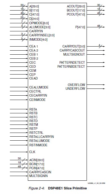
DSP48E1 Primitive
Currently, there is no support for DSP within the F4PGA toolchain. What this essentially means is that the architecture files and routing graphs of all the parts do not contain information about the DSP blocks. These are used for placement and routing of the implemented design on the FPGA fabric. Hence, the toolchain behaves as if there were no DSP resources available on the target board. I need to model the DSP48E1 site using its official documentation and regenerate the routing graph and the architecture file for the targeted board.
First I am modelling only one mode of DSP48E1 (25 x 18 bit multiplier). I will add all the other modes (pre-adding, pattern detection, etc.) in the subsequent weeks. I am referring to the VTR docs and Xilinx documentation for this purpose. dsp48e1.model.xml dsp48e1.pb_type.xml
Updating VPR Libraries
Yosys is used for synthesis in F4PGA. The Yosys-generated primitives need to be tech-mapped to the VPR-compatible ones for subsequent stages. Yosys supports dsp48e1 but VPR doesn't. To make sure there is no instance of dsp48e1 in the Yosys output netlist, "-no_dsp" flags are used in the TCL scripts of the toolchain which invoke Yosys. This makes sure that the RTL design is implemented using LUTs. If we remove the flags, there will be an error during the techmap stage. We need to modify cells_map.v and cells_sim.v to enable technology mapping for dsp48e1. The code below is a part of cells_map.v.
 DSP48E1_VPR #(
    .AREG_0(AREG==0),
       .BREG_0(BREG==0),
       .MASK(MASK),
       .ADREG(ADREG[0]),
       .ALUMODEREG(ALUMODEREG[0]),
       .ACASCREG(ACASCREG[0]),
       .BCASCREG(BCASCREG[0]),
       .CARRYINREG(CARRYINREG[0]),
       .CARRYINSELREG(CARRYINSELREG[0]),
       .DREG(DREG[0]),
       .INMODEREG(INMODEREG[0]),
       .IS_ALUMODE_INVERTED(IS_ALUMODE_INVERTED),
       .IS_INMODE_INVERTED(IS_INMODE_INVERTED),
       .IS_OPMODE_INVERTED(IS_OPMODE_INVERTED),
    .MREG(MREG[0]),
       .OPMODEREG(OPMODEREG[0]),
       .PREG(PREG[0])
    ) _TECHMAP_REPLACE_ (
        .ACOUT(ACOUT),
        .BCOUT(BCOUT),
        .CARRYCASCOUT(CARRYCASCOUT),
        .CARRYOUT(CARRYOUT),
        .MULTSIGNOUT(MULTSIGNOUT),
        .OVERFLOW(OVERFLOW),
        .P(P),
        .PATTERNBDETECT(PATTERNBDETECT),
        .PATTERNDETECT(PATTERNDETECT),
        .PCOUT(PCOUT),
        .UNDERFLOW(UNDERFLOW),
        .A(A),
        .ACIN(ACIN),
        .ALUMODE(ALUMODE),
        .B(B),
        .BCIN(BCIN),
        .C(C),
        .CARRYCASIN(CARRYCASCIN),
        .CARRYIN(CARRYIN),
        .CARRYINSEL(CARRYINSEL),
        .CEA1(CEA1),
        .CEA2(CEA2),
        .CEAD(CEAD),
        .CEALUMODE(CEALUMODE),
        .CEB1(CEB1),
        .CEB2(CEB2),
        .CEC(CEC),
        .CECARRYIN(CECARRYIN),
        .CECTRL(CECTRL),
        .CED(CED),
        .CEINMODE(CEINMODE),
        .CEM(CEM),
        .CEP(CEP),
        .CLK(CLK),
        .D(D),
        .INMODE(INMODE),
        .MULTSIGNIN(MULTSIGNIN),
        .OPMODE(OPMODE),
        .PCIN(PCIN),
        .RSTA(RSTA),
        .RSTALLCARRYIN(RSTALLCARRYIN),
        .RSTALUMODE(RSTALUMODE),
        .RSTB(RSTB),
        .RSTC(RSTC),
        .RSTCTRL(RSTCTRL),
        .RSTD(RSTD),
        .RSTINMODE(RSTINMODE),
        .RSTM(RSTM),
        .RSTP(RSTP)
    );
Adding a DSP test for a 25 x 18 bit multiplier
After making all the above changes and additions to the toolchain, I added a DSP test to see if the toolchain works. I am using the following RTL design source. Notice that I have used structural instantiation instead of behavioural. This is because I want to specifically test 25x18 bit multiplier mode. Values of Inmode, Opmode and Alumode are taken from the reverse-engineered FASM file.
`timescale 1ns / 1ps
module top
  (
    A, B, OUT
  );
   (* IOSTANDARD = "LVCMOS33" *) input wire [24:0] A;
   (* IOSTANDARD = "LVCMOS33" *) input wire [17:0] B;
   (* IOSTANDARD = "LVCMOS33" *) output wire [16:0] OUT;

   DSP48E1 #(
       .AREG(1'b0),
       .BREG(1'b0),
       .MASK(48'b111111111111111111111111111111111111111111111111),
       .IS_ALUMODE_INVERTED(4'b1100),
       .IS_INMODE_INVERTED(5'b11111),
       .IS_OPMODE_INVERTED(7'b1000101),
   )
   dsp25x18(
       .A(A),
       .ACIN(30'b000000000000000000000000000000),
       .ALUMODE(4'b0011),
       .B(B),
       .BCIN(18'b000000000000000000),
       .C(48'b111111111111111111111111111111111111111111111111),
       .CARRYCASCIN(1'b0),
        .CARRYIN(1'b0),
        .CARRYINSEL(3'b000),
        .CEA1(1'b0),
        .CEA2(1'b0),
        .CEAD(1'b0),
        .CEALUMODE(1'b0),
        .CEB1(1'b0),
        .CEB2(1'b0),
        .CEC(1'b0),
        .CECARRYIN(1'b0),
        .CECTRL(1'b0),
        .CED(1'b0),
        .CEINMODE(1'b0),
        .CEM(1'b0),
        .CEP(1'b0),
        .CLK(1'b0),
        .D(25'b0000000000000000000000000),
        .INMODE(5'b00000),
        .MULTSIGNIN(1'b0),
        .OPMODE(7'b0111111),
        .PCIN(48'b000000000000000000000000000000000000000000000000),
        .RSTA(1'b0),
        .RSTALLCARRYIN(1'b0),
        .RSTALUMODE(1'b0),
        .RSTB(1'b0),
        .RSTC(1'b0),
        .RSTCTRL(1'b0),
        .RSTD(1'b0),
        .RSTINMODE(1'b0),
        .RSTM(1'b0),
        .RSTP(1'b0),
        .P(OUT)
   );
endmodule // MULT25X18
We also need an XDC (Xilinx design constraints) file for our design, a part of which is shown below. These files need to be added to CMakeLists.txt after which the environment is rebuilt. We can now run the test and look for any errors that spring up.
set_property PACKAGE_PIN G16 [get_ports {A[23]}]
set_property PACKAGE_PIN C17 [get_ports {A[9]}]
set_property PACKAGE_PIN J17 [get_ports {A[4]}]
set_property PACKAGE_PIN A15 [get_ports {B[9]}]
set_property PACKAGE_PIN U14 [get_ports {OUT[6]}]
set_property PACKAGE_PIN H17 [get_ports {A[14]}]
set_property PACKAGE_PIN J15 [get_ports {A[1]}]
set_property PACKAGE_PIN A14 [get_ports {B[6]}]
set_property PACKAGE_PIN U13 [get_ports {OUT[3]}]
Achievements
Generated FASM files from Vivado-generated bitstreams for different modes of DSP48E1.
Modelled a basic DSP48E1 primitive.
Modified TCL scripts and VPR libraries to enable its support.
Added a DSP test for 25x18 bit mul mode.
All the changes can be found in this Pull-request.
Blockers
The test run fails in the routing stage with multiple warnings and 1 error.
Progress Bar utility is buggy and causes the build to fail.
Targets for the next week
Debug probable causes for the test run failure.
Improve the DSP48E1 primitive by incorporating more modes.