

Introduction
You can find my previous blog here. Earlier I tried running the F4PGA toolchain by using a basic DSP48E1 primitive. I made the necessary changes throughout the toolchain to allow the generation of a bitstream for designs containing DSP instances. I ran into a few errors which I was able to resolve with the help of my mentor. This week I focused on completing the DSP48E1 primitive by referring to its official XILINX documentation.
Architectural Features of DSP48E1
Digital Signal Processing algorithms require many multipliers, adders and accumulators. FPGAs have many dedicated DSP slices that are highly customizable. The figure below shows the internal features of a DSP48E1 block:
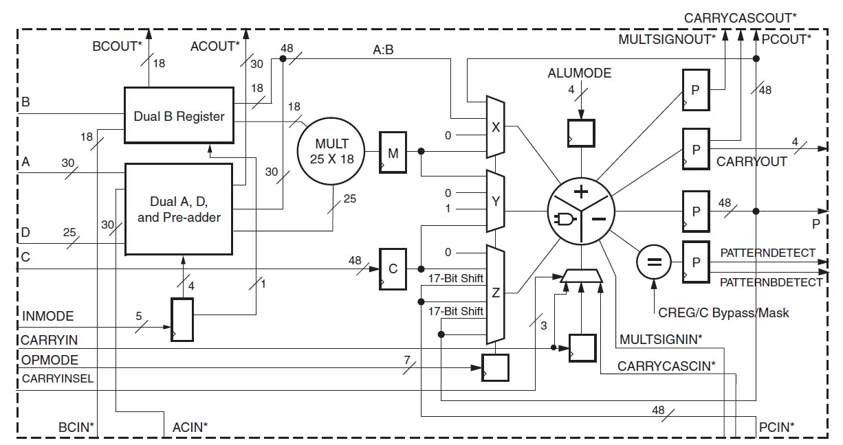
Major features include a 25 × 18 two’s-complement multiplier, 48-bit accumulator (which can also be used as a counter), pre-adder, arithmetic unit (Dual 24-bit or quad 12-bit add/subtract/accumulate), pattern detector and pipelining capabilities. There are also dedicated buses for cascading multiple DSP blocks together. The DSP blocks can be customized to perform a whole range of operations, a few of which are given below:
(A+D)*B+C
(A+D)*B+P>>17+CARRYIN
(ACIN+D)*B+PCIN>>17+CARRYIN
(D-ACIN)*BCIN+P
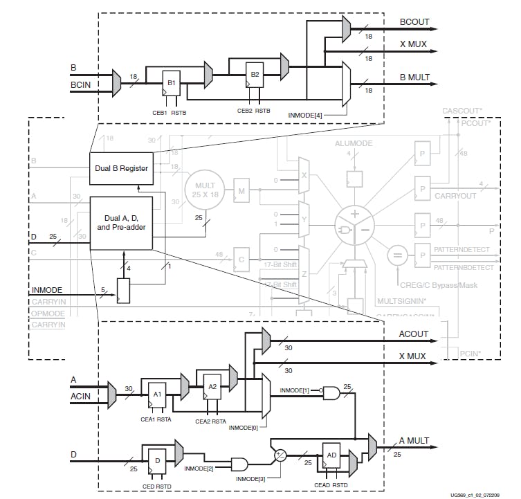
DSP block contains a lot of pipeline registers. Every single register can be bypassed and has an independent clock enable and synchronous reset, thus they can even be configured dynamically at run time. The figure below shows the internal structure of the A and B registers. Notice how each pipeline register can be bypassed using a multiplexer:
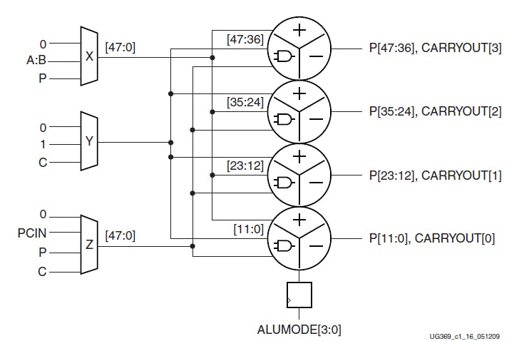
The OPMODE, INMODE and ALUMODE inputs together decide things like the input configuration, operation to be performed, pipelining configuration, etc. Another interesting aspect is that the 48-bit accumulator can be split into smaller data segments where the internal carry propagation between segments is blocked to ensure independent operation for all segments. This is called Single Instruction, Multiple Data (SIMD) Mode:
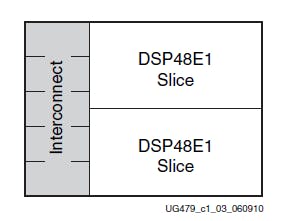
An FPGA can have multiple columns of DSP tiles stacked on top of each other. Each DSP tile has two DSP48E1 slices as shown below. Each DSP48E1 slice has cascade inputs and outputs from its neighbouring DSP48E1 slices along the entire DSP column.
Here I have only outlined some of the major features of the DSP48E1 slice. You can check its documentation for in-depth information about its structure and operation.
VTR Architecture Reference
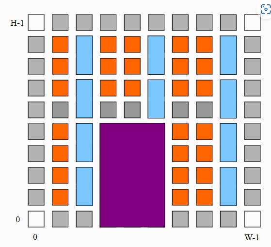
VTR uses an XML-based architecture description language to describe the targeted FPGA architecture. It is used for packing, placement and routing, ultimately generating a FASM file. The architecture file consists of multiple tags defining different parts of an FPGA. There are tags for specifying the i/o pins, the layout of the FPGA grid, the interconnection of different components, delays, etc. The figure below shows an example of an FPGA grid that can be modelled using this method. Each quadrilateral represents a certain kind of tile. They can be CLBs (common logic blocks), RAM slices, I/O banks, DSP blocks, etc. Different sizes of quadrilaterals signify the difference in sizes of these tiles:
Currently, the architecture definitions within the F4PGA toolchain don't include DSP blocks. Hence FPGAs are modelled as if they did not have DSP blocks. Consequently, the VTR cannot perform pack, place and route of DSP slices. I need to model the DSP48E1 primitive using its documentation and update the FPGA architecture description by regenerating the routing graph. I am following the official VTR docs for this purpose.
Designing with the DSP48E1 slice
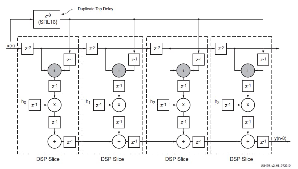
Enabling the support for DSP blocks in the F4PGA toolchain will allow efficient implementation of DSP algorithms used extensively in video broadcasting and wireless communications. FIR filters, interpolators, decimators, etc. can be implemented once the routing graph of a target part in F4PGA contains DSP blocks. The following image shows an 8-tap Even symmetric systolic FIR filter. All the DSP slices are in cascade and don't use fabric routing resources for connections between DSP slices:
More such examples can be found here. Reading the use cases of DSP blocks made me realise the true importance of these resources in an FPGA.
Achievements
Modelled Dual B Reg.
Modelled Dual A, D and pre-adder.
All the changes can be found in this commit.
Blockers
Detailed modelling of DSP48E1 primitive down to each register and multiplexer is taking longer than expected. After consulting with my mentor, I discovered that a simpler higher-level model of the primitive will be sufficient for the toolchain.
Each configuration results in different delay characteristics of the DSP block. I need to map different modes to different VPR cells to achieve this but the total number of configurations is quite large (100+).
Targets for the next week
Complete the remaining architecture description of DSP48E1 primitive.
Incorporate timing information into the DSP primitive.